Roughly half of last week was spent working on the Moo 2.0 Schematic modifications and the other half was spent either on-site or in the lab experimenting with ways to improve the tag rate in mortar. I will first discuss the status update on the concrete deployment project and go into some detail about the Moo 2.0 modifications.
Concrete Deployment Update
Monday morning, Mike and I went over to the house to deploy two additional Moos inside the 3rd course of the sidewall (Moos #29 and #214). Both Moos were placed with the signal antenna sticking slightly out of the cinder block. We found that we were able to get a pretty good tag rate with #214 both before and after the remaining wall got built up. However, we struggled to get a reading from #29 even before more cinder blocks were laid on top. This motivated us to research ways in which we can improve the tag rate inside wet mortar. After obtaining a sample of wet mortar from the construction site, Mike and I ran some additional experiments in the lab to see if you could improve the communication inside mortar. The following google doc summarizes our findings and observations from this experiment: Tin Foil & mortar experiment

Summary of experiment:
- placing tin foil behind the full submerged moo with 4 inch air-gap improved the tag rate from 0 (no reading) to 16 tags/sec (max). First time getting a reading from a completely submerged moo inside wet mortar!
- not able to get a reading when tin foil was placed directly on top of the moo (i.e. no air-gap separation)
- experiment yielded similar results when performed outdoors (with added ambient noise)
This prompted Denis to place two additional (super-capped) moos with tin foil surrounding the inner walls of the two adjacent (non-filled) cinder blocks on the 6th course of the sidewall.
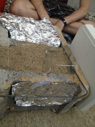
The following day, Mike and I performed some additional experiments outside of the lab using a cinder block filled with wet sand and a sheet of tin foil placed halfway through hole as well as on the two adjacent openings (see picture below). In this orientation with one moo antenna sticking out, we were able to get a tag rate of 19.5 tags/sec.
Later that day, Mike, Denis, and I went back to the house to reposition the readers and map out the moo placement on the front wall. While walking around with the reader and power cords inside my backpack (aka “Ghostbuster pack”) and my laptop in my hands, we were able to scan the moos one-by-one inside the walls for signs of a tag rate. We were able to successfully get a tag rate from the following moos
Rear wall: #23 (max rate of ~6), #17, #26
Note: we observed that the reader antennas performed best in certain orientations and at very specific positions against the wall. Denis placed tape on the walls indicating their orientation. Also, we noticed that certain antenna types worked best with certain moos.
Side wall: #25 (max ~40), #214 (max ~60), and #19 (stray moo)
We repositioned the readers to record #23, #25, and #214 with hopes of catching the curing process.
Update from Mike (on July 20, 2013 at around 1pm):
#214 had a reading of 1.2 tags/sec
#25 has no reading (last seen on 7/17 at 10:06pm)
#23 has a reading of 21.9
——————————————————————————————————————
Moo 2.0 Improvements Update
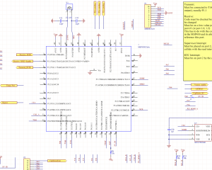
For the rest of the week, I continued to read through the MSP430 Book, Wolverine Datasheet and user guide as well as the F2618 user guide and datasheet to better understand how the MCU functions. I have continued to make modifications to following google doc (Schematic Design Notes) tracking my notes for easier reference later on. Below is a screen capture of the schematic as of this writing.
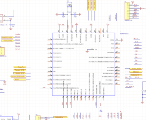
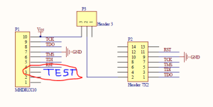
I have placed the connections for power (AVss, DVss, gnd), the crystal oscillator (LFXIN and LFXOUT) along with their external load capacitors (see google doc), and the JTAG connections (TCK, TDO, TMS, TDI, RST, and TEST). Note: the TEST pin is used on the F5969 to enable the JTAG pins. This pin was not required on the F2618 because the MCU’s JTAG pins were dedicated (aka not shared with GPIO pins). We will have to modify the Program header board schematic to accommodate for this additional pin (see below).
As can be seen from the schematic, I still need to route the connections for Transmit, Receive from the RF circuit, ADC inputs (temp, accelerometer, etc.) and the supervisor interrupt. I have begun contacting Jeremy Gummerson with questions regarding the old design as well as suggestions for the new one.